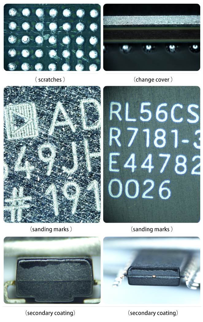
Description:Appearance test means to confirm the number of chips received, inner packaging, humidity indicator, desiccant requirements and appropriate outer packaging.Secondly, the appearance of a single chip is inspected, including: the typing of the chip, the year, the country of origin, whether it is re-coated, the state of the pins, whether there are traces of re-grinding, unidentified residues, and the location of the manufacturer's logo.
Application scope:Determine whether the chip is brand new, refurbished, whether the pins are tinned, oxidized, etc. according to relevant testing standards.
Appearance inspection picture:

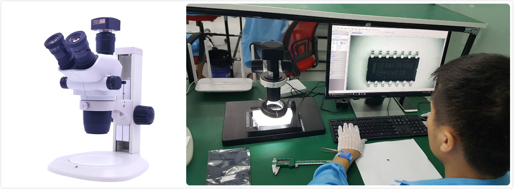
Picture of appearance inspection equipment:

Appearance inspection introduction:
Appearance defect inspection is a very important part of the electronics, precision hardware, printing, plastics and other industries. Both users and manufacturers attach great importance to the appearance of products. Therefore, appearance visual inspection has become very important. One ring.
Contents of appearance inspection:
1. The inspection contents of the package include: scratches, stains, damage, underfilling, spillage, etc.
2. The content of printing inspection includes: typos, offset, missing printing, multiple printing, blur, tilt, displacement, hyphenation, double printing, no fonts, etc.
3. The content of the pin detection includes: missing pins, broken pins, pin spacing, pin width, pin bending, pin span, pin length difference, pin standing height, pin coplanarity , The pin is tilted, etc.
Significance of morphology observation and measurement
① The micro-geometric characteristics of the surface of the material affect many of its technical performance and use functions to a large extent.
②Observing the surface morphology of the material provides convenience for studying the morphology and structure of the sample, and helps to monitor the quality of the product and improve the process.
Application field
Materials, electronics, lead-free soldering, machining, semiconductor manufacturing, aviation, automobiles, ceramics, geology, medicine, metallurgy, etc.
Test process
Sample requirements
Sample requirements for electron microscope observation: non-magnetic or weakly magnetic, non-deliquescent and non-volatile solid samples, less than 8CM*8CM*2CM.
Sample requirements for optical microscope observation: no special requirements.
Test steps
Confirm sample type→confirm inspection specification→observe sample→record observation phenomenon/measurement data evaluation→result evaluation


 Weixin Service

 DouYin
 KuaiShou


