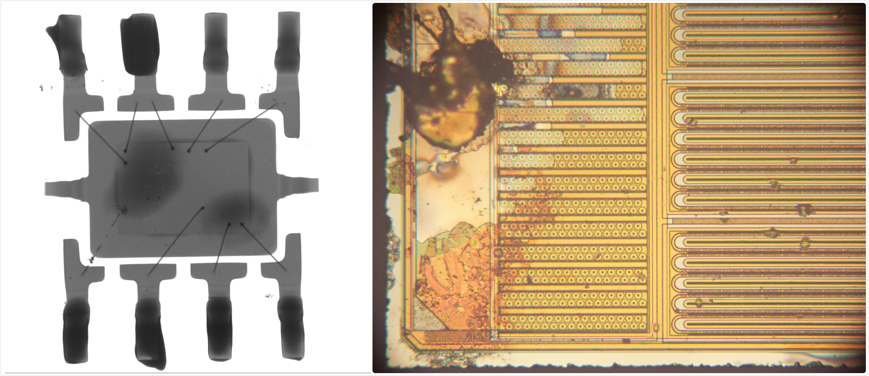
Description:Through professional failure analysis equipment, using various test analysis techniques and analysis procedures to confirm the failure phenomenon of electronic components, distinguish its failure mode and failure mechanism, confirm the final failure cause, and put forward suggestions for improving the design and manufacturing process to prevent Recurring failures.
Application Scope:Analysis of the causes of all failed devices.
Application failure analysis picture:

Basic concepts of failure analysis
1. Failure analysis often requires electrical measurement and the use of advanced physical, metallurgical and chemical analysis methods.
2. The purpose of failure analysis is to determine the failure mode and failure mechanism, and propose corrective measures to prevent the recurrence of this failure mode and failure mechanism.
3. Failure mode refers to the observed failure phenomenon and failure form, such as open circuit, short circuit, parameter drift, functional failure, etc.
4. Failure mechanism refers to the physical and chemical process of failure, such as fatigue, corrosion and overstress.
The significance of failure analysis
1. Failure analysis is a necessary means to determine the failure mechanism of a chip.
2. Failure analysis provides necessary information for effective fault diagnosis.
3. Failure analysis provides necessary feedback information for design engineers to continuously improve or repair the chip design to make it more consistent with the design specifications.
4. Failure analysis can evaluate the effectiveness of different test vectors, provide necessary supplements for production testing, and provide the necessary information basis for verifying the optimization of the test process.
The main steps and content of failure analysis
Unpacking the chip:
Remove the IC encapsulant while keeping the chip function intact, keeping die, bondpads, bondwires and even lead-frame from damage, preparing for the next step of chip failure analysis experiment.
SEM scanning electron microscope/EDX component analysis:
Including material structure analysis/defect observation, element composition routine micro-area analysis, accurate measurement of component size, etc.Probe test: Use micro probes to quickly and easily obtain the internal electrical signals of the IC.
Laser cutting:
Cut a specific area on the circuit or chip with a micro laser beam.
EMMI detection:
The EMMI low-light microscope is a highly efficient failure analysis tool that provides a highly sensitive and non-destructive fault location method that can detect and locate very weak light (visible light and near-infrared light), thereby capturing various Visible light for leakage current caused by component defects or abnormalities.
OBIRCH application (laser beam induced impedance change test):
OBIRCH is often used for high-impedance and low-impedance analysis inside the chip, and line leakage path analysis.Using the OBIRCH method, it is possible to effectively locate defects in the circuit, such as holes in lines and holes under through holes.The high-resistance area at the bottom of the through hole can also effectively detect short circuits or leakage, which is a powerful supplement to the luminescence microscopy technology.
LG LCD hot spot detection:
Using the liquid crystal sensor to detect the molecular arrangement and reorganization of the IC leakage, it shows a patchy image different from other areas under the microscope. Find the leakage area that troubles the designer in the actual analysis (the fault point of more than 10mA).
Fixed-point/non-fixed-point chip grinding:
Remove the gold bumps implanted on the LCD driver chip Pad to keep the Pad intact for subsequent analysis or rebonding.
X-Ray non-destructive detection:
Detect various defects in IC packaging such as layer peeling, bursting, voids, and integrity of wire bonding, possible defects in the PCB manufacturing process such as poor alignment or bridging, open circuit, short circuit or abnormal connection defects, and solder balls in the package Completeness.
SAM (SAT) ultrasonic flaw detection:
Non-destructive inspection of the internal structure of the IC package can effectively detect various damages caused by moisture or heat, such as: o wafer surface delamination, o solder balls, wafers or cracks in the filler, o packaging The pores in the material, o various pores such as the pores in the wafer joint surface, solder ball, filler, etc.


 Weixin Service

 DouYin
 KuaiShou


