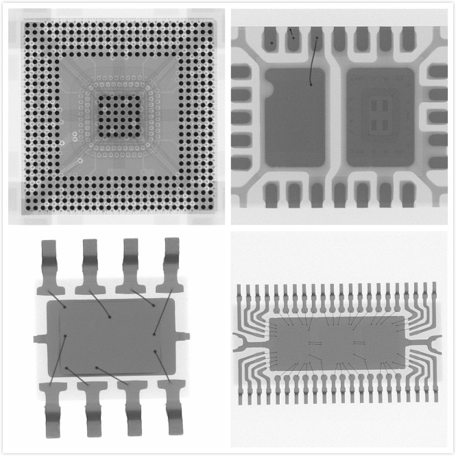
Description:X-ray test is a real-time non-destructive analysis to check the internal hardware components of the component. It mainly checks the lead frame of the chip, wafer size, gold wire bonding diagram, ESD damage and holes. Customers can provide good products for comparison. examine.
Application scope:detection of internal cracks and foreign body defects in metal materials and parts, plastic materials and parts, electronic components, electronic components, LED components, etc., analysis of internal displacements such as BGA, circuit boards, etc.; distinguishing empty welding and virtual welding Wait for BGA welding defect analysis, etc.
X-Ray inspection picture:

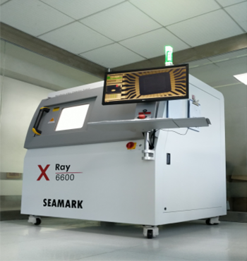
X-Ray inspection equipment picture:

X-Ray inspection introduction:
X-ray (X-ray) detector uses low-energy X-rays without damaging the inspected item to quickly detect the inspected object.The high-voltage impact target is used to generate X-ray penetration to detect the internal structure quality of electronic components, semiconductor packaging products, and the welding quality of various types of solder joints of SMT.
X-Ray inspection content:
1) Defect inspection in IC packaging, such as: layer peeling, burst, void and integrity inspection of bonding;
2) Defects that may occur in the printed circuit board manufacturing process, such as: poor alignment or bridging and open circuit;
3) SMT solder joint void phenomenon detection and measurement;
4) Defect inspection for open circuit, short circuit or abnormal connection that may occur in various connection lines;
5) Integrity inspection of solder balls in solder ball array packaging and chip-on-chip packaging;
6) Inspection of plastic materials with higher density or holes in metal materials;
7) Chip size measurement, wire arc measurement, and component tin area ratio measurement.
X-Ray detection steps:
Confirm the test location and requirements of the sample type/material→Put the sample into the X-Ray fluoroscope inspection table for X-Ray fluoroscopy inspection→Picture judgment analysis→Mark the defect type and location.
X-Ray inspection items:
1. Integrated circuit packaging process inspection: layer peeling, cracking, void and wire bonding process;
2. Printed circuit board manufacturing process inspection: wire offset, bridging, open circuit;
3. Weldability inspection of surface mount technology: inspection and measurement of solder joint voids;
4. Check the connection line: open circuit, short circuit, abnormal or bad connection defect;
5. Integrity inspection of solder balls in solder ball array packaging and chip-on-chip packaging;
6. High-density plastic material cracking or metal material inspection;
7. Chip size measurement, wire arc measurement, and component tin area ratio measurement.


 Weixin Service

 DouYin
 KuaiShou


