Application of X-ray in chip defect detection
Date:2022-04-01 17:02:07 Views:1252
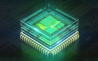
Chip is the carrier of integrated circuit, which is divided by wafer. There are traces of chip in our smart phones, computers, televisions, automobiles and air conditioners. As an electronic component with high integration and precise structure, and the continuous emergence of various new packaging technologies, the requirements for circuit assembly quality are higher and higher. The chip X-ray detection equipment mainly uses the X-ray generated in the X-ray inspection machine to irradiate the inside of the chip. The X-ray has strong penetration and can image after penetrating the chip. The internal structure fracture of the chip can be seen at a glance. The main feature of using X-ray to detect the chip is that there is no damage to the chip itself. Therefore, this detection method is also called nondestructive testing.
Principle of chip defect detection using X-ray Technology
In the process of chip detection, the X-ray detection equipment launched by domestic professional X-ray detection equipment manufacturers can improve the chip detection efficiency. X-ray detection equipment uses the X-ray emission tube to generate x-rays, which pass through the chip sample and generate a projection on the image receiver. Its high-definition imaging system can be magnified by 1000 times, so as to show the internal structure of the chip more clearly, and provide an effective detection means for improving the "one-time pass rate" and striving for the goal of "zero defect".
In fact, in the face of chips with very realistic appearance but defective internal structure on the market, it is obviously impossible to distinguish them by the naked eye. Only under the X-ray detection can they show the "original shape". Therefore, the X-ray detection equipment provides sufficient guarantee for the chip detection of products in the production process of electronic products and plays an important role.
_20220401170131_292.jpg)
Characteristics of X-ray testing:
1) The coverage rate of process defects is as high as 97%. Defects that can be checked include: virtual welding, bridging, tombstone, insufficient solder, pores, missing components, etc. In particular, X-ray can also check hidden devices, such as BGA and GSP solder joints.
2) Higher test coverage. You can check where you can't check the naked eye and online test. For example, it is judged that PCBA is faulty, and it is suspected that the inner layer of PCB is damaged, and X-ray can be checked quickly.
3) The test preparation time is greatly shortened.
4) Defects that cannot be reliably detected by other test methods can be observed, such as false soldering, porosity and poor molding.
5) Double sided and multilayer boards only need to be checked once.
6) Provide relevant measurement information to evaluate the production process. Such as the thickness of solder paste, the amount of solder under the solder joint, etc.
X-ray detection technology has brought new changes to SMT production detection methods. It can be said that it is also a good choice for manufacturers who are eager to further improve the production process level, improve the production quality and find the breakthrough of circuit component faults in time. I hope it can help you. We will bring more wonderful content later. The company's testing services cover: electronic component testing and verification, IC authenticity identification, product design and material selection, failure analysis, function testing, factory incoming material inspection, tape braiding and other testing items. Welcome to call Chuangxin testing. We will serve you wholeheartedly.


 Weixin Service

 DouYin
 KuaiShou


