What are the main failure analysis methods of "summary" components?
Date:2021-09-23 15:22:40Views:2714
Failure analysis is an important part of product reliability engineering. Failure analysis is widely used to determine the causes of production problems in the process of development and production, identify reliability related failures in the process of testing, and confirm the on-site failure mechanism in the process of use. In the development stage of electronic components, failure analysis can correct errors in design and development and shorten the development cycle; In the production, testing and use stage of electronic components, failure analysis can find out the failure causes of electronic components and the responsible party causing the failure of electronic components. What are the main failure analysis methods? Let's have a look.
1、 C-sam (ultrasonic scanning microscope) is a non-destructive examination:
The test contents include:
1. Lattice structure, impurity particles, inclusions and precipitates inside the material
2. Internal cracks
3. Delamination defect
4. Voids, bubbles, voids, etc.

2、 X-ray (X-ray testing) is a non-destructive inspection:
X-ray uses the cathode ray tube to produce high-energy electrons to collide with the metal target. In the process of impact, due to the sudden deceleration of electrons, the lost kinetic energy will be released in the form of X-ray. For the position where the sample cannot be observed by appearance, the contrast effect generated by the change of light intensity after X-ray penetrating substances with different densities can form an image, which can show the internal structure of the object to be measured, and then the problem area inside the object to be measured can be observed without damaging the object to be measured.
The test contents include:
1. Observe electronic components such as semiconductors, resistors, capacitors and small PCB printed circuit boards with different packages such as dip, SOP, QFP, QFN, BGA and flipchip
2. Observe the chip size, quantity, stacking die and wire binding inside the device
3. Observe chip crack, uneven dispensing, wire breakage, grounding, internal bubbles and other packaging defects, as well as solder ball cold welding, false welding and other welding defects
3、 SEM scanning electron microscope / EDX energy dispersive X-ray apparatus(material structure analysis / defect observation, element composition, conventional micro area analysis, accurate measurement of component size), SEM / EDX (morphology observation and composition analysis) scanning electron microscope (SEM) can directly use the material properties of the sample surface materials for micro imaging. EDX is realized by analyzing the characteristic X-ray wavelength and intensity of elements emitted by the sample. The elements contained in the sample are determined according to the different characteristic X-ray wavelengths of different elements. The content of elements in the sample can be determined by comparing the intensity of spectral lines of different elements. Usually, EDX combined with electron microscope (SEM) can be used to analyze the micro composition of samples.
The test contents include:
1. Material surface morphology analysis and micro area morphology observation
2. Analysis of material shape, size, surface, section and particle size distribution
3. Surface morphology observation, film roughness and film thickness analysis of film samples
4. Nano size measurement and marking
5. Qualitative and quantitative analysis of micro components
4、 Emmi low light microscope.For fault analysis, emission microscope (Emmi) is a very useful and efficient analysis tool. It mainly detects photons emitted from the IC. In IC components, EHP (electron hole pairs) recombination will emit photons. For example, when a bias voltage is applied to the p-n junction, the electrons of the N well are easy to diffuse to the P well, and the holes of P are easy to diffuse to N, and then EHP recombination is made with the holes at the P end (or the electrons at the N end).
The test contents include:
1. P-n interface leakage; P-n interface collapse
2. Hot electron of saturation region transistor
3. Photon excitation generated by oxide leakage current
4. Latch up, gate oxide defect, junction leakage, hot carriers effect, ESD and other problems
5、 FIB line modification, tangent line, tangent point observation, TEM sample preparation, precision thickness measurement, etc
FIB (focused ion beam) is to accelerate the ion beam generated by liquid metal ion source through ion gun, focus and irradiate it on the sample surface to generate secondary electron signal and obtain electron image. This function is similar to SEM (scanning electron microscope), or peel off the surface atoms with strong current ion beam to complete micro and nano surface morphology processing.
The test contents include:
1. Chip circuit modification and layout verification
2. Cross section analysis
3.Probing Pad
4. Fixed point cutting
6、 Probe station / probe test, the probe table is mainly used in semiconductor industry and photoelectric industry. Testing of integrated circuits and packages. It is widely used in the research and development of precision electrical measurement of complex and high-speed devices to ensure quality and reliability, and reduce the research and development time and the cost of device manufacturing process.
The test contents include:
1. Small connection point signal leading out
2. Failure analysis and failure confirmation
3. Confirmation of electrical characteristics after modification of FIB circuit
4. Wafer reliability verification
ESD / latch up ESD / latch up utility test (some customers conduct these two reliability tests before the chip flows into the client, and some customers think of screening good chips for inspection after failure). These have mentioned most common methods. There are some necessary sample processing procedures before failure analysis.

7、 Take die and decap, grind, remove golden ball, de gold bump, remove layer, dye, etc, some also need corresponding instruments and machines. SEM can view the die surface, Sam and X-ray to observe the internal conditions of the package and delamination failure. Decap refers to opening the seal, also known as opening the cover and cap. It refers to local corrosion of the fully encapsulated IC, so that the IC can be exposed, while maintaining the integrity of the chip function, and keeping die, bond pads, bond wires and even lead frame from damage, so as to prepare for the next chip failure analysis experiment, facilitate observation or other tests (such as FIB and Emmi). After decap, the function is normal.
The test contents include:
1. IC unsealing (front / back) QFP, QFN, sot, to, dip, BGA, cob, etc
2. Sample thinning (except ceramics and metals)
3. Laser marking
8、 Acid decap, also known as chemical unsealing, is a device that uses chemical methods, i.e. concentrated sulfuric acid and fuming nitric acid to remove plastic sealing materials。 By etching the plastic covered on the chip surface with acid, the chip in any plastic IC package can be exposed. The plastic removal process is fast and safe, and produces a clean and corrosion-free chip surface.
The test contents include:
1. Chip unsealing (front / back)
2. IC etching and plastic package removal
9、 RIE is a kind of dry etching, the principle of this etching is that when a high-frequency voltage (RF, radio frequency) of 10 ~ 100MHz is applied between the plate electrodes, an ion sheet with a thickness of hundreds of microns will be generated, in which the sample is placed, and the ions impact the sample at a high speed to complete the chemical reaction etching, which is RIE (reactive ion etching).
The test contents include:
1. For isotropic and anisotropic etching of materials using fluorine based chemistry, including carbon, epoxy resin, graphite, indium, molybdenum, nitrogen oxide, photoresist, polyimide, quartz, silicon, oxide, nitride, tantalum, tantalum nitride, titanium nitride, tungsten titanium and tungsten
2. Etching of device surface pattern
10、 Grinding machine, suitable for high precision(light mirror, SEM, TEM, AFM, etc) semi-automatic preparation, grinding and polishing of samples, modular preparation, grinding, parallel polishing, precision angle polishing, location polishing or a combination of several methods.
The test contents include:
1. Fine grinding and polishing of section
2. Chip process analysis
3. Finding the failure point

11、 The cutting machine can preset programs to locate and cut various materials of different sizes, and can automatically cut materials at high speed to improve sample production.The micro processing system can adjust the cutting distance, force, sample input ratio and automatic feed ratio of the stepping motor according to the material and thickness of the material.
The test contents include:
1. Obtain the standard section of the sample through the cold buried injection molding of the sample
2. Precision cutting of small samples
12、 Metallographic microscope can be used to observe the appearance of devices and the surface shape, size, structure and defects of failure parts.The metallographic microscope system organically combines the traditional optical microscope with the computer (digital camera) through photoelectric conversion. It can not only make microscopic observation on the eyepiece, but also observe the real-time dynamic image on the computer (digital camera) display screen. The computer-based metallographic microscope can edit, save and print the required pictures.
The test contents include:
1. Sample appearance and morphology inspection
2. Metallographic and microscopic analysis of prepared samples
3. Search for various defects
13、 Stereomicroscope, also known as solid microscope or anatomical microscope.It is a binocular microscope with positive stereoscopic sense, which can observe objects from different angles and make both eyes cause stereoscopic sense. The observation body does not need to be processed and manufactured. It can be observed directly under the lens with illumination. The imaging is vertical and easy to operate and dissect. The diameter of the field of view is large, but the magnification of the observation object is required to be less than 200 times.
The test contents include:
1. Sample appearance and morphology inspection
2. Observation and analysis of sample preparation
3. Inspection and analysis after opening the cap of the package
4. Transistor spot welding and inspection
14、 IV automatic curve measuring instrument to verify and measure the electrical properties, parameters and characteristics of semiconductor electronic components.Such as voltage current. In the IC failure analysis process, I / V curve measurement is often the second step of non-destructive analysis (appearance inspection is the first step), which shows the importance of curve measurement.
The test contents include:
1.Open/Short Test
2.I/V Curve Analysis
3.Idd Measuring
4. Powered leakage test
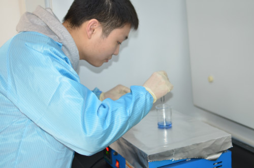
15、 The high and low temperature test chamber is suitable for high and low temperature reliability test of industrial products.Check the performance indexes of parts and materials of electronic and electrical engineering, automotive electronics, aerospace, marine weapons, colleges and universities, scientific research institutions and other related products under the condition of cyclic change of high temperature and low temperature (alternating).
The test contents include:
1. High temperature storage
2. Low temperature storage
3. Temperature and humidity storage
According to the results of failure analysis, the component manufacturer shall improve the design and production process of components, the component user shall improve the circuit board design, and improve the testing, test premise and procedure of components or the whole machine, and even replace the component suppliers with different grid based on this. Therefore, failure analysis is of great significance to speed up the development of electronic components and improve the yield and reliability of components and complete machines.
The failure process is a very complex process. In particular, there are many kinds of mechanical equipment structures, the structures are generally complex, the hinge coupling between systems and between systems is strong, the working conditions of metal components are bad and complex, there are many doubtful points after failure, and the analysis is difficult, which requires the failure analysts to have a certain depth of theoretical knowledge and a wide range of knowledge, At the same time, it should also have rich practical experience.


 Weixin Service

 DouYin
 KuaiShou


