How to do chip failure analysis? Basic steps of failure analysis and brief introduction of common equipment
Date:2021-04-27 15:57:00Views:1792
With the continuous improvement of people's requirements for product quality and reliability, failure analysis is becoming more and more important. In recent years, it has been popularized from military industry to ordinary enterprises. It is generally based on the failure mode and phenomenon, through analysis and verification, simulate and reproduce the failure phenomenon, find out the cause of failure, and dig out the failure mechanism. Determining the chip failure mechanism provides necessary information for effective fault diagnosis. It also provides necessary feedback for design engineers to continuously improve or repair the chip design and make it more consistent with the design specifications. It can also evaluate the effectiveness of different test vectors, provide necessary supplements for production testing, and provide necessary information basis for verification test process optimization. The failure analysis of electronic components has become a very important part.
Failure analysis is the process of diagnosing the failure mechanism and causes of electronic components, and it is the only way to improve the reliability of electronic components. Components from design to production to application may fail, so failure analysis runs through the whole life cycle of electronic components. Therefore, it is necessary to find out the cause of failure, determine the failure mode, and put forward corrective measures to prevent the same failure mode and failure mechanism from recurring on each component and improve the reliability of components.

Basic steps of failure analysis
Chip unsealing:
Remove the IC sealant, keep the chip function intact, and keep die, bond pads, bond wires and even lead frame from damage, so as to prepare for the next chip failure analysis experiment.
SEM / SEM / EDX composition analysis:
Including material structure analysis / defect observation, element composition, conventional micro area analysis, accurate measurement of component size, etc. Probe test: quickly and conveniently obtain the internal electrical signal of IC with microprobe.
Laser cutting:
A micro laser beam is used to cut the line or a specific area on the upper layer of the chip.
Emmi detection:
Emmi low light level microscope is a highly efficient failure analysis tool, which provides a highly sensitive and non-destructive fault location method. It can detect and locate very weak luminescence (visible light and near-infrared light), so as to capture the visible light of leakage current caused by various component defects or abnormalities.
OBIRCH application (laser beam induced impedance value change test):
OBIRCH is often used for internal high impedance and low impedance analysis and line leakage path analysis. Using OBIRCH method, defects in the circuit can be located effectively, such as holes in lines and holes under through holes. The high resistance area at the bottom of the through hole can also effectively detect short circuit or leakage, which is a powerful supplement to the luminescence microscopy technology.
LG LCD hot spot detection:
The liquid crystal is used to sense the arrangement and reorganization of molecules at the IC leakage, showing a mottled image different from other areas under the microscope, so as to find the leakage area (fault point exceeding 10mA) that puzzles the designer in the actual analysis.
Fixed / non fixed point chip grinding:
Remove the gold bump planted on the LCD driver pad and keep the pad intact for subsequent analysis or rebinding.
X-ray nondestructive testing:
Detect various defects in IC package, such as layer peeling, burst, cavity and wire integrity, possible defects in PCB process, such as poor alignment or bridging, open circuit, short circuit or abnormal connection, and tin ball integrity in package.
Sam (SAT) ultrasonic flaw detection:
It can carry out non-destructive detection on the internal structure of IC packaging, and effectively detect various damages caused by water vapor or heat energy, such as: O delamination of wafer surface, O cracks in tin ball, wafer or glue filling, O pores in packaging materials, O various holes, such as holes at wafer joint surface, tin ball, glue filling, etc.
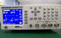
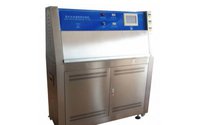
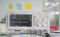
Common equipment and detailed uses for failure analysis are shown in the figure below:


 Weixin Service

 DouYin
 KuaiShou


