Common failure analysis methods and processes of chip
Date:2021-04-26 16:41:00Views:2621
Generally speaking, the failure of integrated circuits is inevitable in the process of development, production and use. With the continuous improvement of people's requirements for product quality and reliability, failure analysis is becoming more and more important. Chip failure analysis can help integrated circuit designers find design defects, mismatch of process parameters or improper design and operation. The common methods of chip failure analysis are no more than those processes. The most important thing is to rely on various advanced and accurate electronic instruments. The following contents are mainly elaborated from these two aspects, hoping to be helpful to you.
_20210426164037_326.jpg)
IFailure analysis process:
1. Appearance inspection, identify crack, burn mark and other problems, and take photos.
2. Non destructive analysis: mainly use Xray to check the internal structure, and CSAM to check whether there is delamination
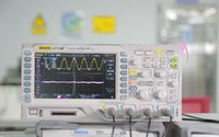
3. Electrical test: main tools, multimeter, oscilloscope, etc
4. Conduct destructive analysis: mechanical decap or chemical decap, etc
IICommon analysis methods:
Common analysis methods of chip:
1. X-ray nondestructive testing can be used for testing
Various defects in IC packaging, such as layer peeling, burst, cavity and wire integrity
Possible defects in PCB manufacturing process, such as poor alignment or bridging
Defects of open circuit, short circuit or abnormal connection
Solder ball integrity in packaging
2. Sat ultrasonic flaw detector / scanning ultrasonic microscope
It can carry out non-destructive detection on the internal structure of IC package, and effectively detect various damages caused by water, gas or heat, such as:
Wafer surface delamination
Cracks in solder balls, wafers or filler
Pores inside the packaging material
Various holes, such as holes at wafer joint surface, tin ball, glue filling, etc
3. SEM scanning electron microscope / EDX energy dispersive X-ray apparatus
It can be used for material structure analysis / defect observation, element composition, conventional micro area analysis, and accurate measurement of component size
4. Three common leakage current path analysis methods: Emmi low light level microscope / OBIRCH laser beam induced impedance change test / LC liquid crystal hot spot detection
Emmi LLM is used to detect abnormalities caused by ESD, latch up, I / O leakage, junction defect, hot electrons, oxide current leakage, etc.
OBIRCH is often used for high and low impedance analysis and line leakage path analysis Using OBIRCH method, defects in the circuit can be located effectively, such as holes in lines and holes under through holes. High resistance area at the bottom of through hole, etc; It can also effectively detect short circuit or leakage, which is a powerful supplement to luminescence microscopy.
LC can detect the specific location of chip failure caused by ESD and EOS stress damage.
5. Probe station / probe test probe test can be used to directly observe the internal signal of IC
6. ESD / latch up ESD / latch up utility test
7. FIB circuit modification
FIB focused ion beam can directly cut, connect or jumper metal wires Compared with re - flow verification, FIB tool is used to verify the modification of circuit design, which has obvious advantages in time and cost
According to the introduction of chip failure analysis laboratory, it can carry out testing according to international, domestic and industrial standards, carry out comprehensive testing from bottom chip to actual products, from physics to logic, and provide chip preprocessing, side channel attack, optical attack, intrusive attack, environment, voltage burr attack, electromagnetic injection, radiation injection, physical security, logic security Function, compatibility, multipoint laser injection and other safety detection services. At the same time, it can carry out failure analysis and detection services to simulate and reproduce the failure of intelligent products and find out the failure causes, mainly including probe station, reactive ion etching (RIE), micro leakage detection system (Emmi), X-ray detection, defect cutting observation system (FIB system), etc.
In addition to the common methods, there are other failure analysis methods, such as atomic force microscope AFM, secondary ion mass spectrometry Sims, time of flight mass spectrometry TOF-SIMS, transmission electron microscope TEM, field emission electron microscope, field emission scanning auger probe, X-ray photoelectron spectroscopy XPS, l-i-v test system, energy loss X-ray microanalysis system, etc., but these items are not very commonly used.


 Weixin Service

 DouYin
 KuaiShou


