What is ultrasonic inspection? Difference between X-ray and ultrasonic testing
Date:2023-03-15 16:04:59Views:636
Ultrasonic testing is abbreviated as UT, also known as ultrasonic testing. It uses ultrasonic technology for testing, and is one of five conventional nondestructive testing methods. Common flaw detection methods for flaw detection test include: X-ray flaw detection, ultrasonic flaw detection, magnetic particle flaw detection, penetrant flaw detection (dye flaw detection), eddy current flaw detection γ Radiographic inspection, fluorescent inspection and other methods. To help you understand, the following content is organized by Chuangxin Testing Network for your reference.
Basic principle of ultrasonic flaw detection
There are many kinds of ultrasonic flaw detectors, but in the actual flaw detection process, the pulse reflection ultrasonic flaw detector is the most widely used. Generally, in uniform materials, the existence of defects will cause the discontinuity of materials, which often leads to the inconsistency of acoustic impedance. From the reflection theorem, we know that ultrasound will reflect at the interface of two different acoustic impedance media, and the size of reflected energy is related to the difference of acoustic impedance of the media on both sides of the interface and the orientation and size of the interface. Pulse reflection ultrasonic flaw detector is designed according to this principle.
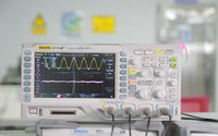
At present, most of the portable pulse reflection ultrasonic flaw detectors are in A-scan mode. The so-called A-scan display mode means that the abscissa of the display is the propagation time or distance of the ultrasonic wave in the tested material, and the ordinate is the amplitude of the ultrasonic reflected wave. For example, there is a defect in a steel workpiece. Because of the existence of this defect, an interface between the defect and the steel material is formed between different media. The acoustic impedance between the interfaces is different. When the emitted ultrasonic meets this interface, it will reflect, and the reflected energy will be received by the probe. A reflected wave will be displayed at a certain position in the abscissa of the display screen, This position of the abscissa is the depth of the defect in the tested material. The height and shape of the reflected wave vary with different defects, reflecting the nature of the defect.
_20230315160334_730.jpg)
Main characteristics of ultrasonic flaw detection
(1) When the ultrasonic wave propagates in the medium, it has the characteristics of reflection on different interfaces. If the defect is encountered and the size of the defect is equal to or greater than the ultrasonic wave length, the ultrasonic wave is reflected back on the defect, and the flaw detector can display the reflected wave; If the size of the defect is even smaller than the wavelength, the sound wave will bypass the ray and cannot be reflected;
(2) The directivity of wave sound is good. The higher the frequency is, the better the directivity is. It radiates into the medium with a very narrow beam, and it is easy to determine the location of defects.
(3) The propagation energy of ultrasonic wave is large. For example, the propagation energy of ultrasonic wave with frequency of 1MHZ (100 Hz) is equal to 1 million times that of sound wave with the same amplitude and frequency of 1000HZ (100 Hz).
Comparison between ultrasonic flaw detection and X-ray flaw detection
Compared with X-ray flaw detection, ultrasonic flaw detection has the advantages of higher flaw detection sensitivity, short cycle, low cost, flexibility, convenience, high efficiency and harmless to human body; The disadvantage is that the working surface is required to be smooth, experienced inspectors are required to identify the types of defects, and the defects are not intuitive; Ultrasonic flaw detection is suitable for inspection of parts with large thickness.
The above is the relevant content of ultrasonic flaw detection organized by the core detection team. I hope it can help you. Our company has a team of professional engineers and industry elites, and has three standardized laboratories with an area of more than 1800 square meters, which can undertake various test projects such as electronic component testing and verification, IC authenticity identification, product design and material selection, failure analysis, functional testing, factory incoming material inspection and tape weaving.


 Weixin Service

 DouYin

 KuaiShou

